
The burger that understood EMC
In 1984 McDonald's launched a burger whose defining feature was not the burger. It was the box. The McDLT shipped in a two-compartment styrofoam clamshell: one side carried the hot stuff, the beef patty and the toasted bun, and the other carried the cool stuff, lettuce, tomato and the crisp top bun. You kept them apart the whole way to the table and folded them together at the last possible second. The pitch was simple: keep the hot side hot, and the cool side cool.
I think about that burger more than is strictly healthy, because it remains the best intuitive explanation of mixed-signal grounding I have ever come across, and nobody in McDonald's marketing department meant it that way.
The antenna you didn't mean to build
Start with the thing that actually fails you: a radiated-emissions scan, RE102 in a shielded room, the receiver lighting up at some clock harmonic while you stand there wondering where it got out.
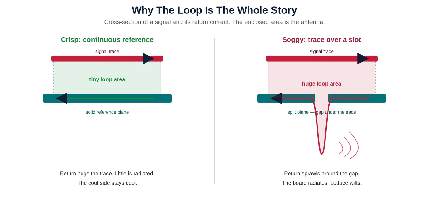
Every current that leaves a driver has to come back. The outbound trace and its return path form a loop, and a loop carrying high-frequency current is an antenna whether you drew it as one or not. To a first approximation the radiated field from a small loop grows with the current, with the enclosed loop area, and with the square of the frequency. Double the loop area and you double the problem; double the clock and you quadruple it. On a ruggedized box that has to pass in a vehicle or an aircraft, that loop is the difference between a clean sweep and a week with a near-field probe.
The trace you were worried about is rarely the culprit; the return current is, and it doesn't go where you assume. At DC it spreads out and takes the path of least resistance. At the frequencies that show up on a radiated-emissions scan it takes the path of least inductance, which is the copper directly beneath the signal trace, because hugging the trace is what keeps the loop area small. A solid reference plane does this for you, for free, on every layer transition, right up until you take the copper out from under the signal. Take it away and the return current has to go find another way home, and it will not pick the way you wanted.
The two-compartment box: splitting the ground
So why would anyone deliberately cut a slot in a perfectly good plane? Because digital return currents are loud. A processor or FPGA dumps sharp, broadband switching current into the reference on every edge. If that noisy return flows through the same copper your 24-bit ADC is using as its definition of "zero volts," then zero volts is no longer zero: it has the digital hash riding on it, and every quiet analog measurement inherits that hash as error.
The instinct, a reasonable one, is to give the sensitive analog section its own clean compartment: its own region of reference that the digital return currents are kept out of. Hot side, cool side. That is a split, or partitioned, ground.
The one rule: never let the sides touch (except where you say so)
A split reference is only as good as your discipline about crossing it, and this is exactly where good engineers turn a clever idea into a failed scan. The return current still needs continuous copper beneath every single trace. Route one clock line straight across the moat and the return current simply cannot follow it; the copper isn't there. So it detours all the way around the end of the slot, opening up a loop the size of the gap. Congratulations: you've built an antenna, and you've conveniently tuned it to your clock and its harmonics.
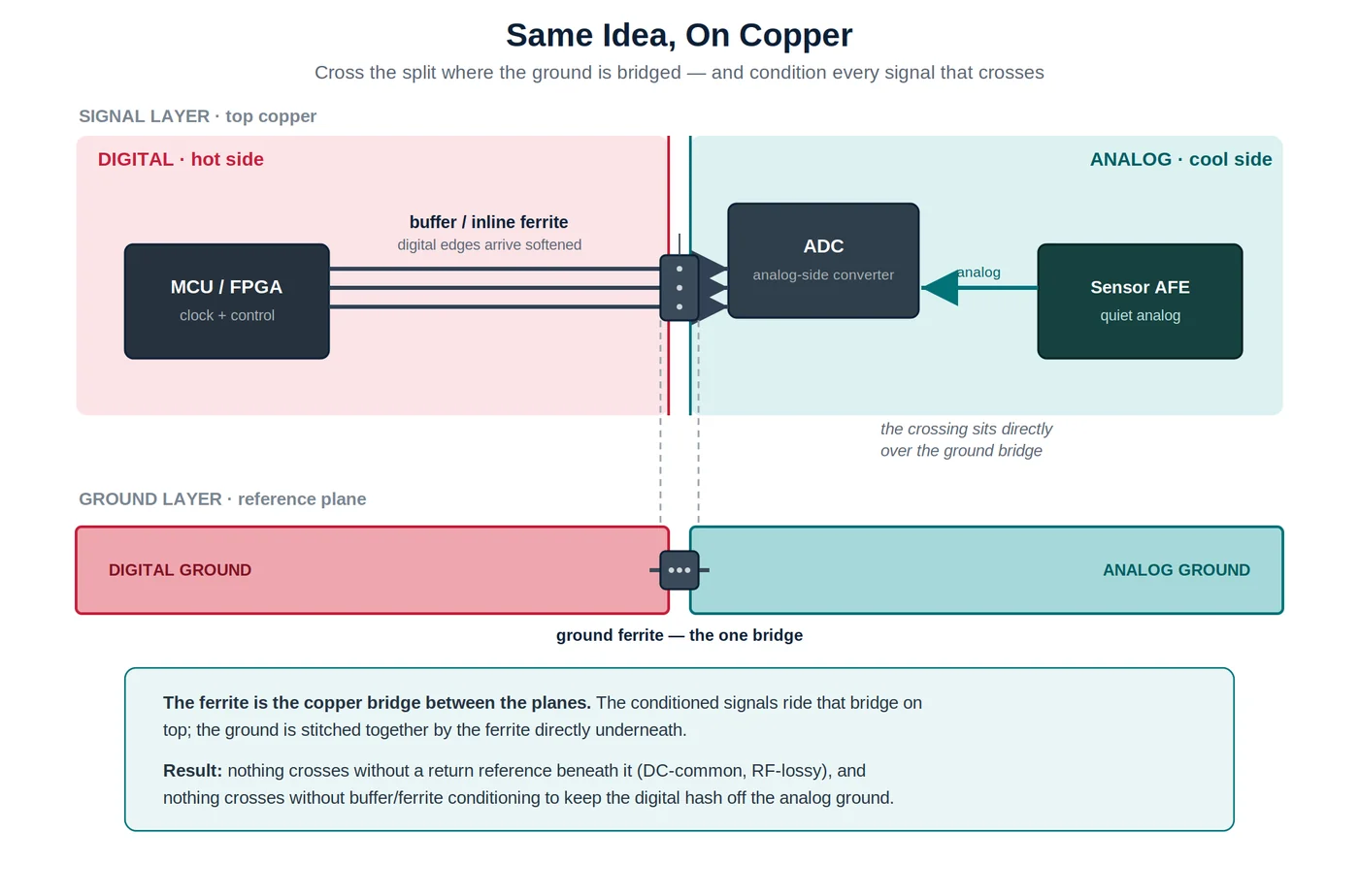
The McDLT rule is the same rule: you may combine the hot and cool sides, but only at the moment and place of serving. On a board that means putting the crossing and the bridge in the same spot. Tie the two ground planes together with a single ferrite directly beneath the point where the control lines cross, so the return current always has copper underneath it: no orphaned return, no detour, no loop. Then condition the lines that actually cross: run them through a buffer or isolation register, or a series ferrite, so the digital edges arrive softened instead of as raw hash.
The picture to hold in your head is two layers stacked: the conditioned signals ride a copper bridge on top, the ferrite stitches the ground planes together underneath, and the two sit one directly above the other. Nothing crosses without a reference beneath it, and nothing crosses without conditioning in series.
The ferrite hinge: one bridge, on purpose
If the two reference regions are completely isolated, nothing stops them from drifting to different potentials, which is its own flavor of bad. So they need to share a DC reference without giving digital RF energy a comfortable path into the analog world. A ferrite bead does precisely this. It looks like a near-short at DC and low frequencies, so the two grounds agree on where zero is, but it becomes lossy and high-impedance at RF, commonly hundreds of ohms across the tens-to-hundreds-of-megahertz range, so high-frequency noise that tries to cross gets absorbed instead of conducted. Place one bead, at one point, right next to the converter. That is your fold-at-serving: the single sanctioned hinge between the compartments.
It helps to stop picturing the bead as an inductor and start picturing it as a frequency-controlled resistor. Down at DC and the low megahertz it's nearly nothing, a few milliohms, basically a wire. Up where the trouble lives it turns resistive and lossy, often a few hundred ohms, and it burns that energy as heat instead of passing it along. That resistance is the property you're actually buying.
Put one in the path of a fast, noisy edge and it rolls the corners off: it stretches the rise and fall, pulls amplitude out of the high harmonics, and damps the ringing that would otherwise keep the line resonating long after the transition. The slower edge is the whole point. You're handing the system a little settling time, enough that the return current comes home through the copper, under the trace, in a tight loop, instead of leaving its high-frequency components to go find a big parasitic loop and radiate out through the air.
Assemble before serving
The slogan was always quietly good engineering advice. Keep the hot side hot: contain your digital return currents where they belong. Keep the cool side cool: protect the analog reference from the hash. And combine the two only at the place and moment you designed for: one bridge, beside the converter, on purpose.
Do that and the board passes its scan and the lettuce stays crisp. Do the opposite, and a soggy sandwich and a failed emissions test turn out to be the same disappointment expressed in different units. The McDLT is gone. The grounding lesson outlived the packaging. Fold responsibly.
Field notes
- Plan the return, not just the trace. Every signal needs continuous reference copper directly beneath it.
- If you split the reference, never route a trace across the gap. The return current can't, so it detours and radiates.
- Cross domains at one defined point, ideally under the data converter that legitimately bridges both.
- Tie the references with a single ferrite bead (or one 0 Ω link): low impedance at DC, high impedance at RF. One bead, one place.
- When in doubt, don't split. A solid plane with analog and digital in their own regions beats a botched moat. Split only deliberately: the datasheet calls for it, or there's a real isolation boundary.
How this was written
This started as a conversation. The engineering (the return-current intuition, the bench scars, and the calls on what actually matters) comes from twenty-five years of doing this work and failing my share of emissions scans. I wrote it with Claude, Anthropic's AI assistant, which helped me organize the argument, sharpen the prose, and draw the figures. The McDLT analogy is mine, and I stand by it. Any errors are mine too; the lettuce metaphors are negotiable.
References and further reading
- Henry W. Ott, Electromagnetic Compatibility Engineering, John Wiley & Sons, 2009: return-current paths, ground partitioning, and why a continuous plane often beats a split one.
- Howard W. Johnson and Martin Graham, High-Speed Digital Design: A Handbook of Black Magic, Prentice Hall, 1993: high-frequency return current follows least inductance under the trace; loop area drives radiation.
- Walt Kester, James Bryant and Mike Byrne, MT-031: Grounding Data Converters and Solving the Mystery of "AGND" and "DGND", Analog Devices, 2009.
- Paul Brokaw and Jeff Barrow, AN-345: Grounding for Low- and High-Frequency Circuits, Analog Devices: current seeks the path of least impedance, not just least resistance.
- Mark I. Montrose, EMC and the Printed Circuit Board: Design, Theory, and Layout Made Simple, IEEE Press, 1999: plane construction, slots, and keeping return loops small.
- MIL-STD-461G, Requirements for the Control of Electromagnetic Interference Characteristics of Subsystems and Equipment, U.S. Department of Defense, 11 December 2015: the RE102 radiated-emissions regime.